MOSFET Breakout board Hookup Guide
This hookup guide is not only limited to the MOSFET breakout board, here you can learn basics of MOSFET, so that you can build your own circuit in a breadboard/ Protoboard with components we are providing or use if you have some with you. Check below the contents we covered in this tutorial:
-
MOSFET BASICS
-
Hardware Needed
-
MOSFET Breakout PCB Introduction
-
PCB SilkScreen
-
Gate Control Circuit Schematics
-
Jumper Settings
-
PCB Assembly
-
Heatsink Assmebly
-
References
MOSFET BASICS
Most of you have heard of BJT and MOSFET but still you have doubts regrading MOSFET, here we are covering some basics of MOSFET before going to the breakout board details. MOSFET stands for “metal-oxide semiconductor field-effect transistor”. It is a special type of field-effect transistor (FET). Its gate input is electrically insulated from the main current carrying channel and is therefore also called as an “Insulated Gate Field Effect Transistor” or “IGFET”. Unlike BJT which is ‘current controlled’, the MOSFET is a voltage controlled device. The MOSFET has “gate“, “Drain” and “Source” terminals instead of a “base”, “collector”, and “emitter” terminals in a bipolar transistor. By applying voltage at the gate, it generates an electrical field to control the current flow through the channel between drain and source, and there is no current flow from the gate into the MOSFET. Unlike the BJT, the FET is a unipolar device since it functions with the conduction of electrons alone for the N-channel type or on holes alone for a P-channel type.
Hope now things are little clear to you now, but this is not enough, so we had covered types of MOSFET as well, refer the types below:
- N-Channel (NMOS) or P-Channel (PMOS)
- Enhancement or Depletion mode
N-Channel – For an N-Channel MOSFET, the source is connected to ground. To turn the MOSFET on, we need to raise the voltage on the gate. To turn it off we need to connect the gate to ground.
P-Channel – The source is connected to the power rail (Vcc). In order to allow current to flow the Gate needs to be pulled to ground. To turn it off the gate needs to be pulled to Vcc.
Depletion Mode – It requires the Gate-Source voltage ( Vgs ) applied to switch the device “OFF”.
Enhancement Mode – The transistor requires a Gate-Source voltage ( Vgs ) applied to switch the device “ON”.
Despite the variety, the most commonly used type is N-channel enhancement mode. There are also “Logic-Level” and “Normal MOSFET”, but the only difference is the Gate-Source potential level required to drive the MOSFET. Refer the symbols in the diagram below to distinguish the types of MOSFET.

MOSFET TYPES
Now consider the following points while connecting the load/Heatsink to the MOSFET:
- Because load has resistance, which is basically a resistor. For N-channel MOSFET put the load at the Drain side and Source is usually connected to GND. If load is connected at the source side, the Vgs will needs to be higher in order to switch the MOSFET, or there will be insufficient current flow between source and drain than expected
- For P-Channel MOSFET put the load at the source side and drain is usually connected to GND.
- Typically the heat sink on the back of a MOSFET is connected to the Drain! If you mount multiple MOSFETs on a heat sink, they must be electrically isolated from the heat sink! It’s good practice to isolate regardless in case the heat sink is bolted to a grounding frame.
| MOSFET type | VGS = +ve | VGS = 0 | VGS = -ve |
|---|---|---|---|
| N-Channel Depletion | ON | ON | OFF |
| N-Channel Enhancement | ON | OFF | OFF |
| P-Channel Depletion | OFF | ON | ON |
| P-Channel Enhancement | OFF | OFF | ON |
Hardware Needed:
 MOSFET Breakout Board | 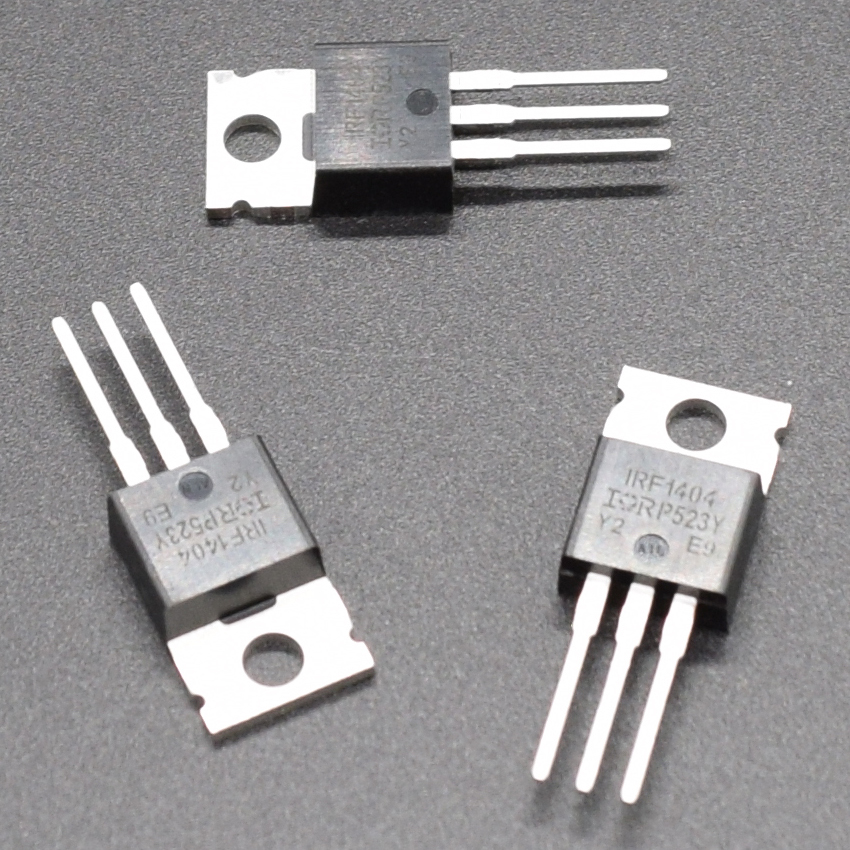 N Channel MOSFET (IRF1404) | 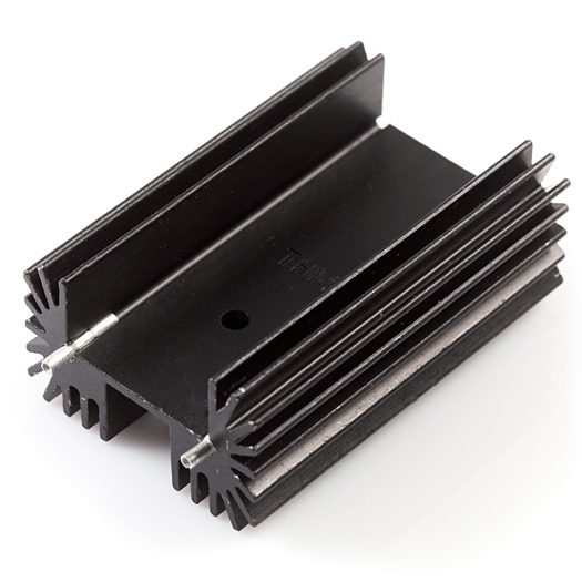 Heatsink -Multiwatt Package |
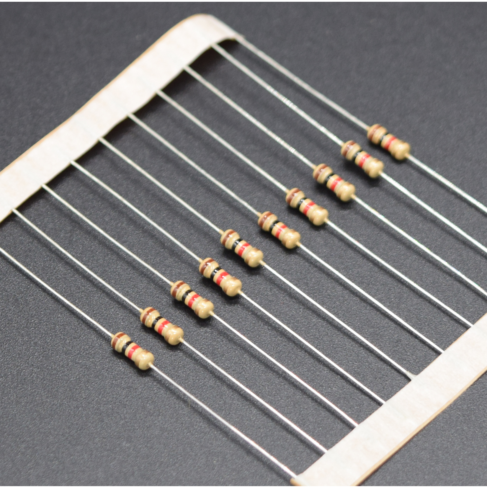 1KΩ Resistor | 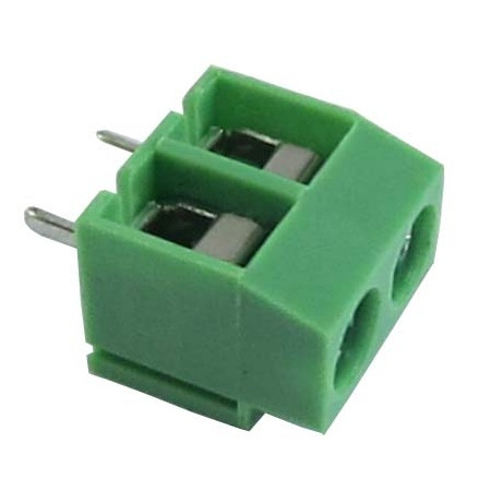 Screw Terminal- 2pin (5mm) | 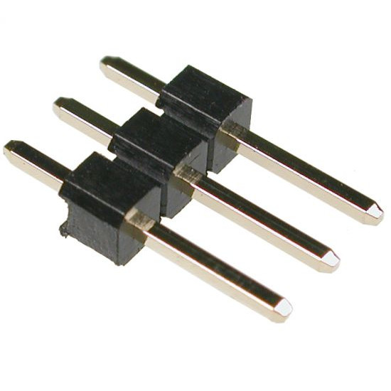 Male Header 40 x 1 |
MOSFET Breakout PCB Introduction:
This basic is enough for now, to getting started with MOSFET. There are many more things which you can do with MOSFET, we did not covered all the things in details here, but we will recommend you to start using MOSFET in most of the circuits to understand its uses in various applications, only practice makes man perfect, so this is what we are expecting from you that you will build something really cool projects using MOSFET. Now its time to go in details of MOSFET breakout board. Refer the board shown in the Image below:
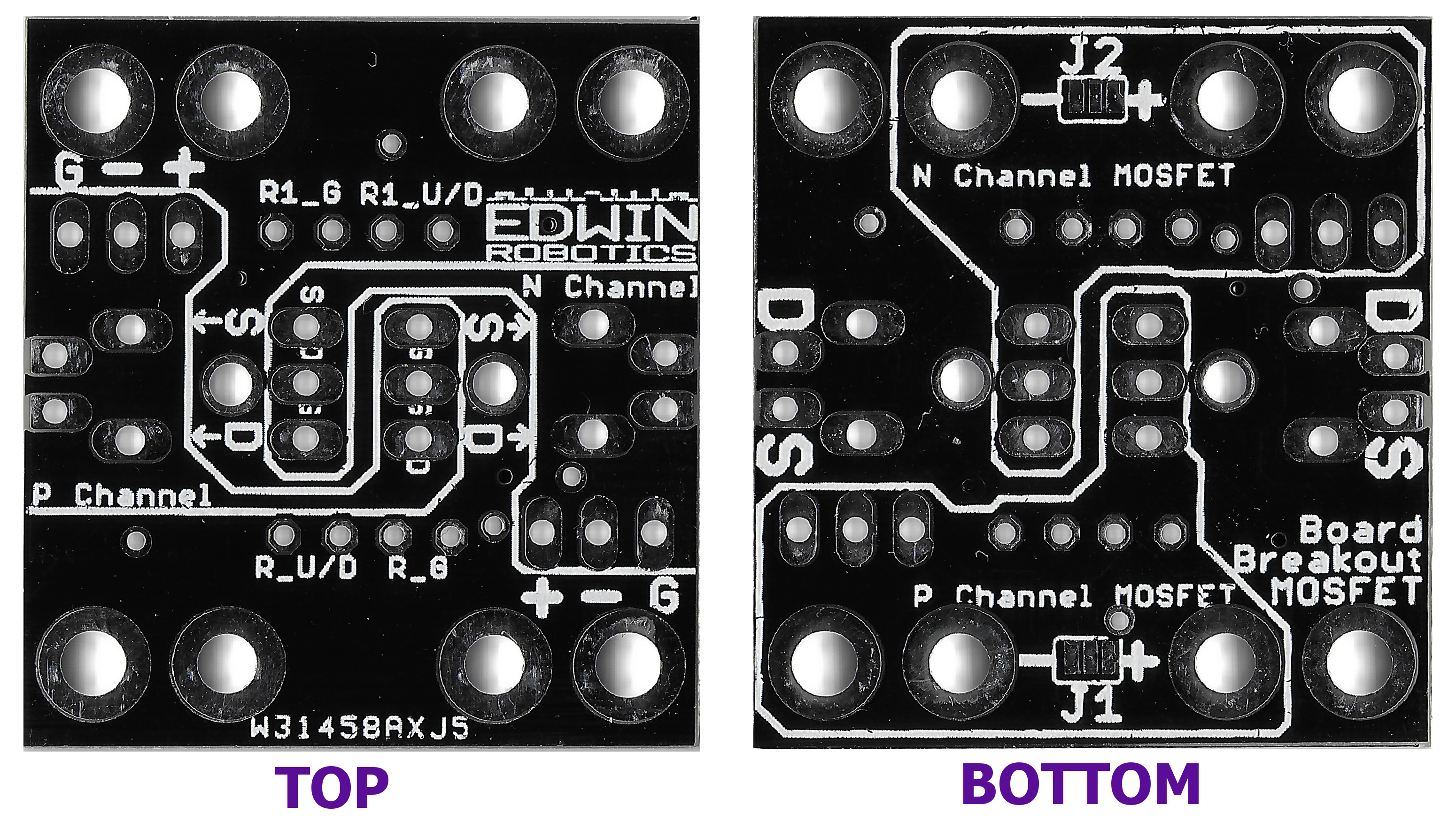
MOSFET BREAKOUT PCB
PCB SilkScreen:
Now if you notice, then you can see the silkscreen at the bottom and the top will distinguish between P Channel side and N channel Side. You only need to solder the parts which are dedicated for that specific channel, i.e if you are willing to use just N channel Enhancement type MOSFET in your project, then all you need to do is to solder the parts needed only for N channel, which you can easily distinguish by referring the silkscreen. We had highlighted the TOP side silkscreen in the following image to distinguish between the two channel side.
N Channel / P Channel
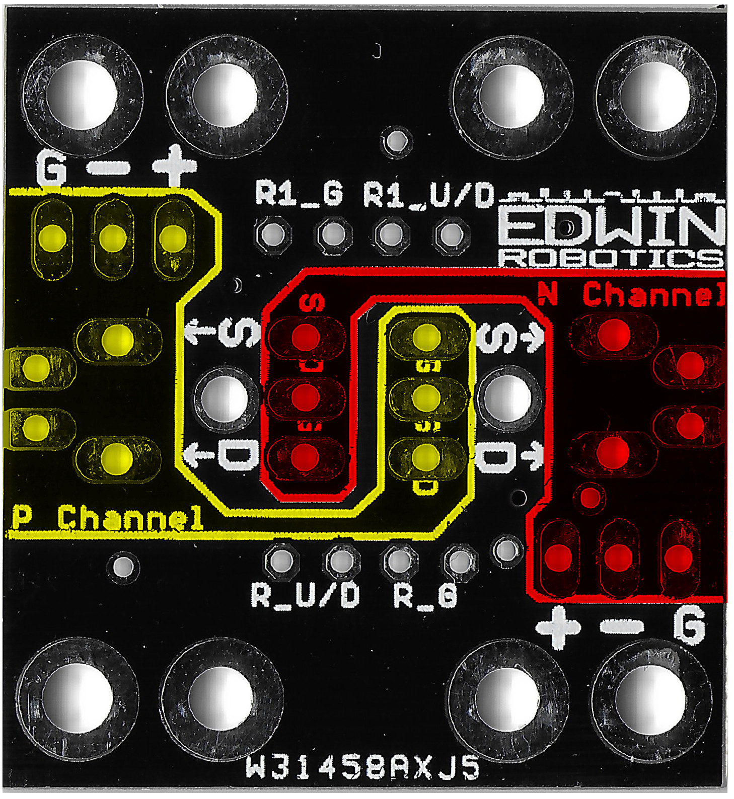
You can refer the following image to see which resistors refer to which channel, this you can easily distinguish, if you refer the bottom silkscreen.
N Channel/ P Channel Resistors
Gate Control Circuit Schematics:
We had added the Pull_Up / Pull_Down Resistor for the Gate, this feature is disabled by default, but if you need you can use this feature in your circuit by enabling the jumper J1/J2. Refer the below Schematics for better idea of the circuit.
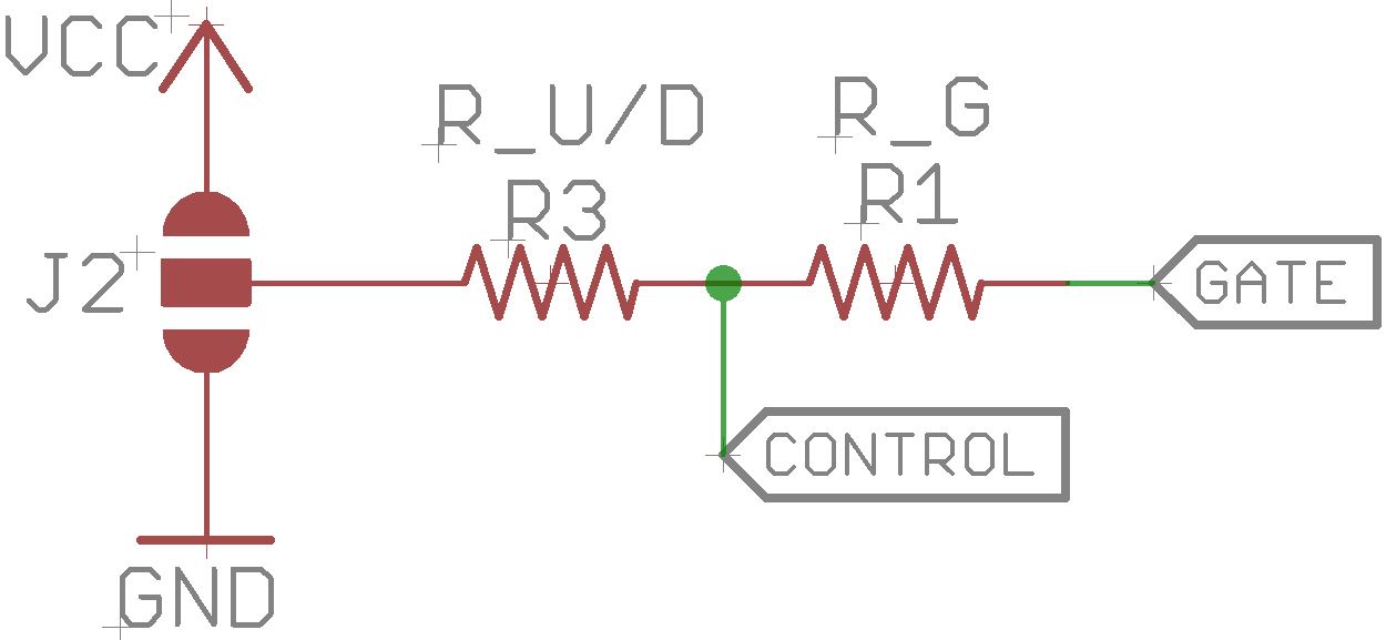
Gate Circuit Schematics
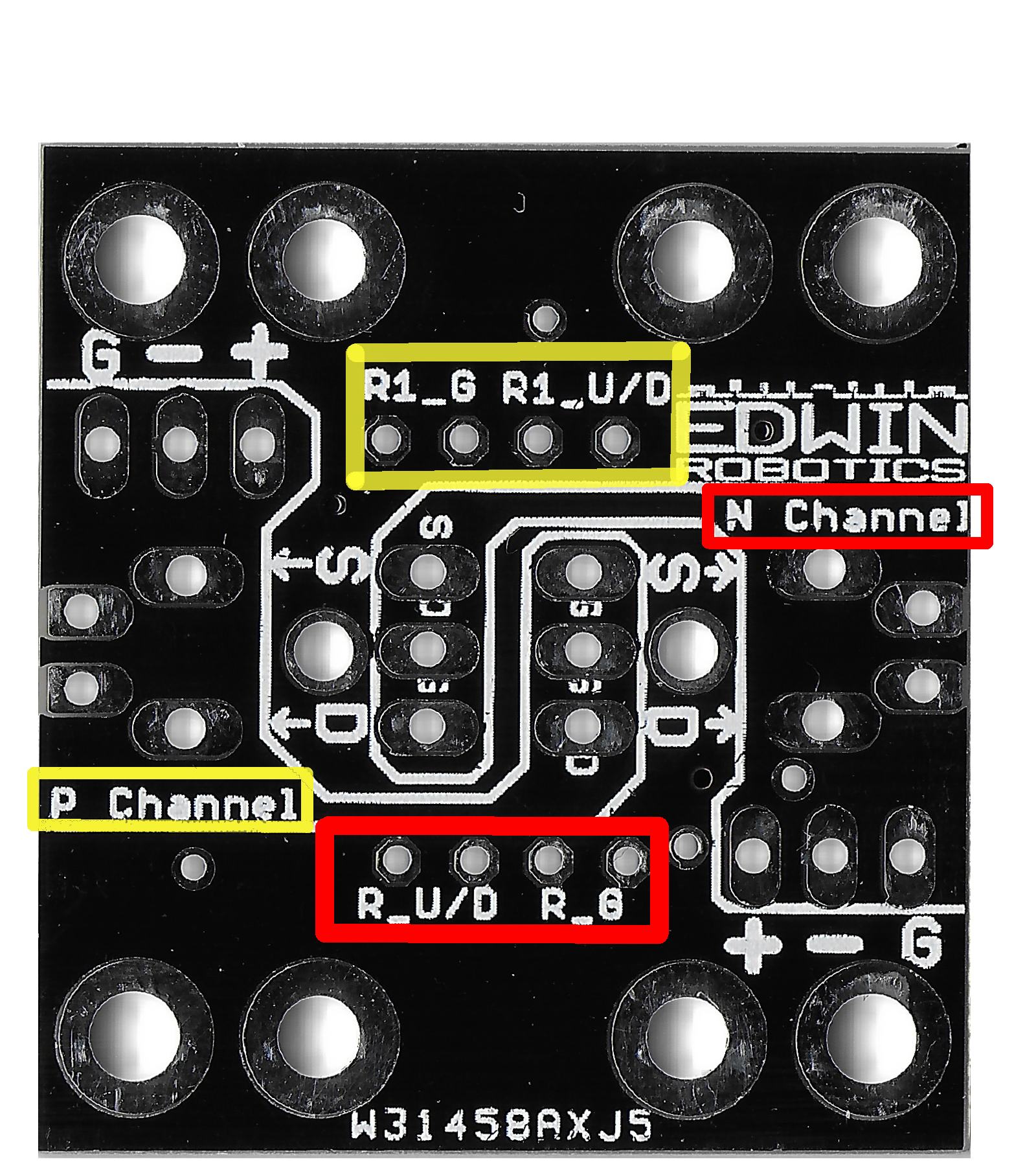
You can see in the following images we had highlighted the pull_up/ pull_down resistors.
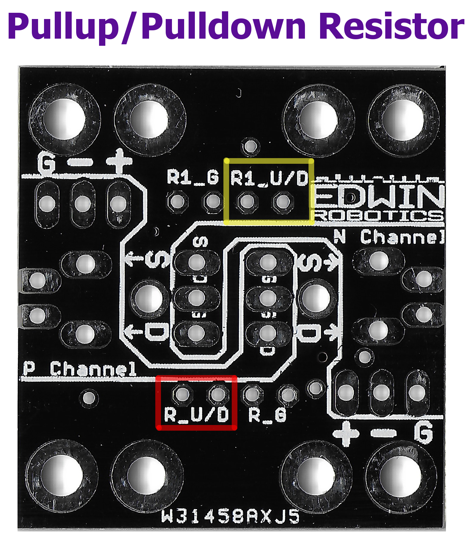
Gate Control Resistors
Jumper Settings:
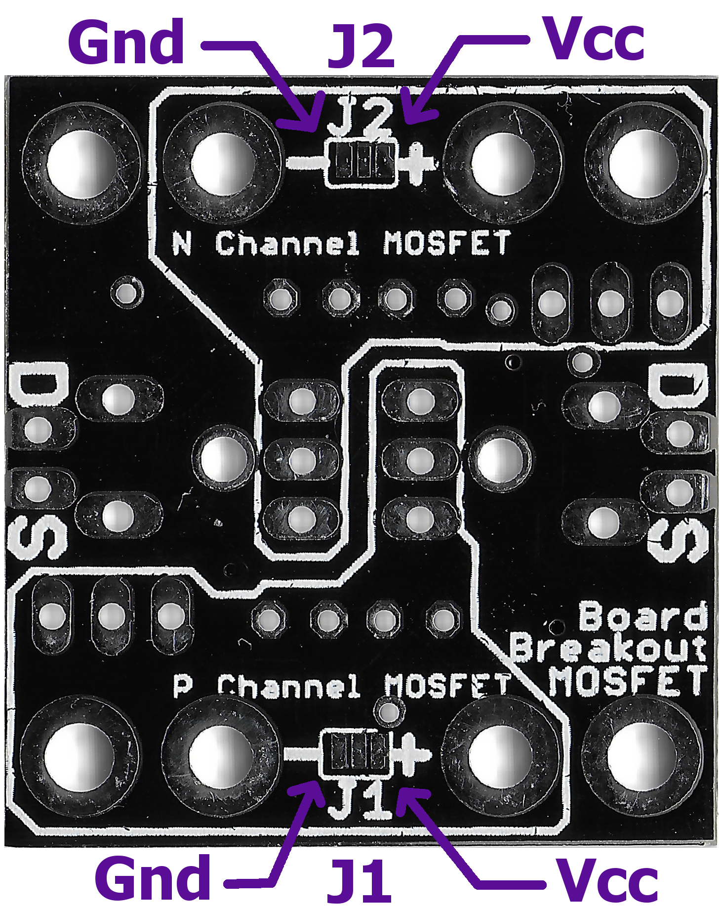
These Pull-Up/Down Resistors (R_U/D) is disabled by default and can be enabled by adding solder to the Jumper Pads J1 for P-Channel and Jumper Pads J2 for N-Channel, the Vcc and Ground side is indicated in the Silkscreen. Its a 2-Way Jumper thus center pad is the main path and you need to apply solder either to “+” or “-“, so make sure to solder only required logic for each jumper, i.e either Vcc or ground. In case you need to disable this feature from the circuit, just remove the solder from the pads you applied. You can see the J1 and J2 Jumper in the following image and the + and – indication against its pad.
Jumper Pads
Note: Do not Solder all the three pads of the jumper together, this will create a short between Vcc and GND.
Refer the below table for jumper selection chart:
CHANNEL | RESISTOR | +(Vcc) | -(GND) |
|
| J1 | P | R1_U/D | Pullup | Pulldown |
| J2 | N | R_U/D | Pullup | Pulldown |
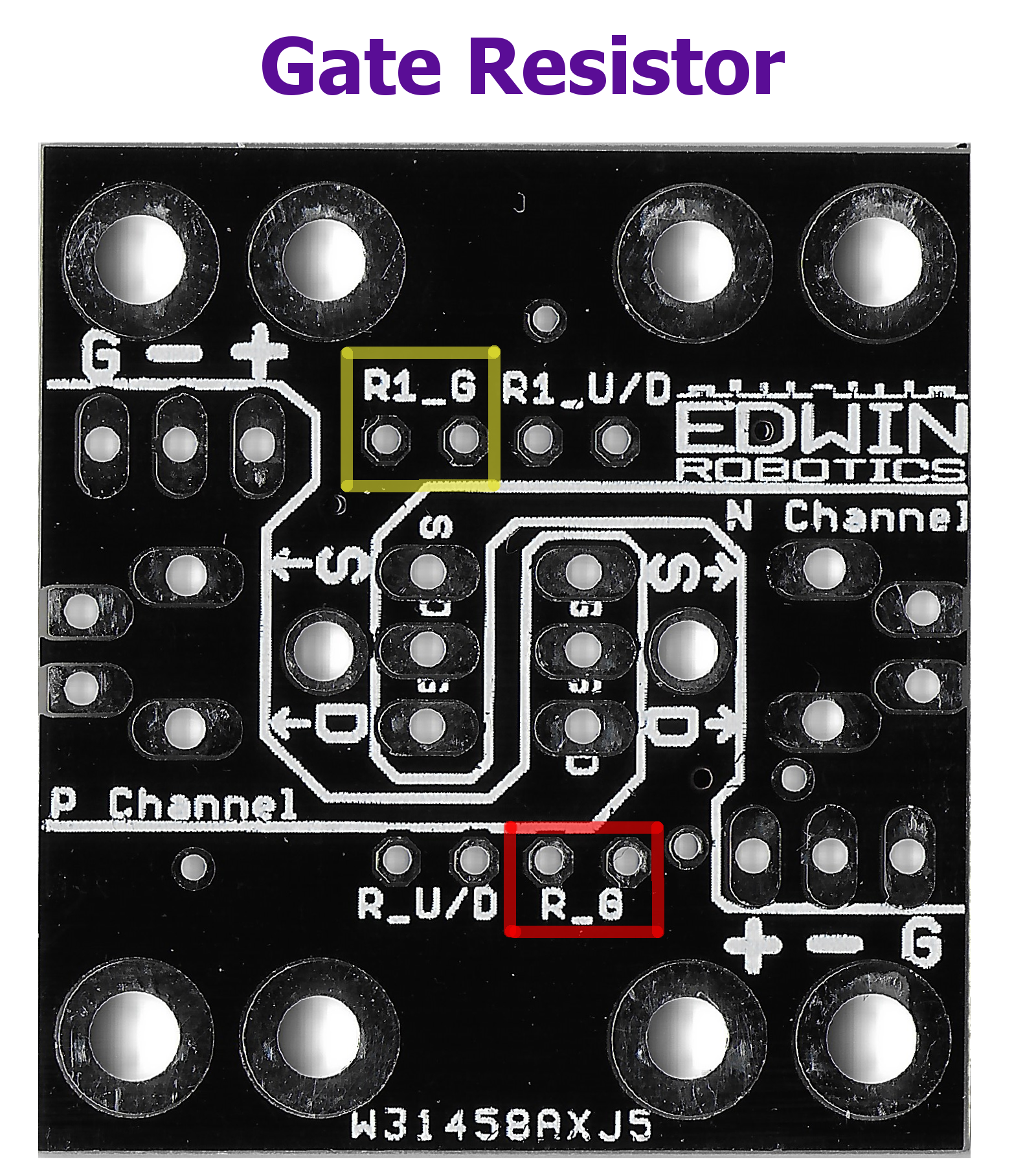
You can ignore these R_U/D and R1_U/D resistor in the breakout board, if you don’t need pull_up/Down Feature. Now if you notice the Gate schematics you can see that the control signal is passed via Gate Resistor, so you need to solder this in your breakout PCB to get the circuit working, if you don’t want any Gate resistors, you can solder the 0Ω Resistor in the R_G / R1_G. We had Provided some standard values of resistors with this breakout board, so you don’t need to worry much about it, all you need to do is, to solder the resistors as per your requirement. Refer the below image for the Gate resistors slot in the Breakout board.
Gate current limit
Note: MOSFET will not work if R_G / R1_G Gate Resistor is left open, atleast you must solder 0Ω Resistor or short the slot with solder/Wire.
PCB Assembly:
The Drain and Source pins are indicated clearly on the TOP/BOTTOM Silkscreen, this can be accessed either with screw terminal or with male/female Headers, you can solder whichever you need. You need to solder three pin header for Gate, Gnd, Vcc pins as well, so as to control the MOSFET from microcontroller or any other circuit. Make sure to use the Gate Control header of the same channel as that of MOSFET. Refer the legend and the diagram below for the N- Channel MOSFET assembly:

Legend
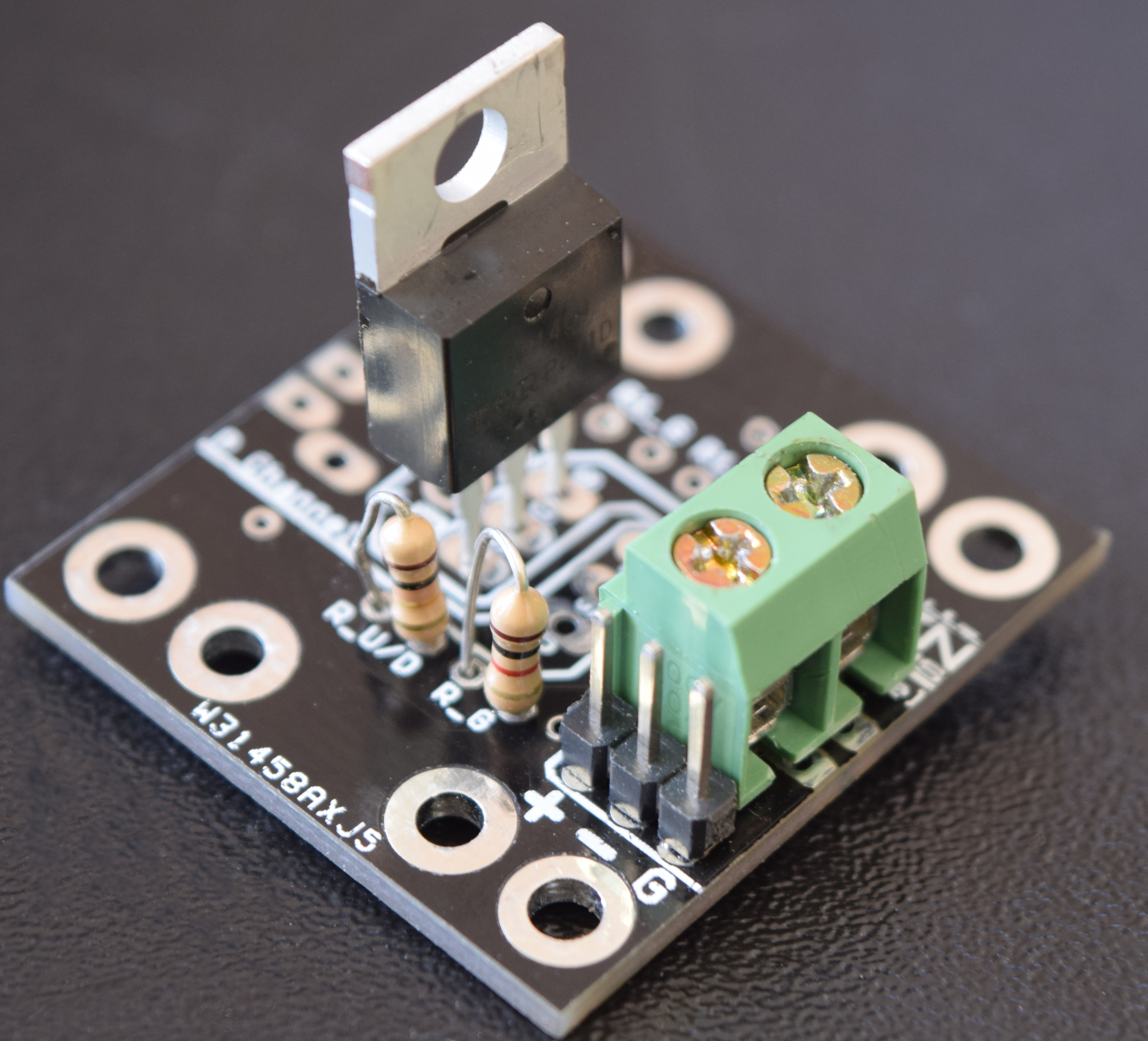
N Channel MOSFET Assembly
Heatsink Assmebly:
The board supports one N Channel and one P-Channel MOSFET at the same time, since both channels have its own sets of resistors, headers and screw terminal slot, make sure that all the things are properly connected. For the high current application your MOSFET will heat up like crazy, thus you need to add heatsink to provide cooling to the MOSFET, we had provided Heatsink Slot to be soldered on board for both type of MOSFET, refer the following image on how to use heatsink with MOSFET:

Heatsink Multiwatt
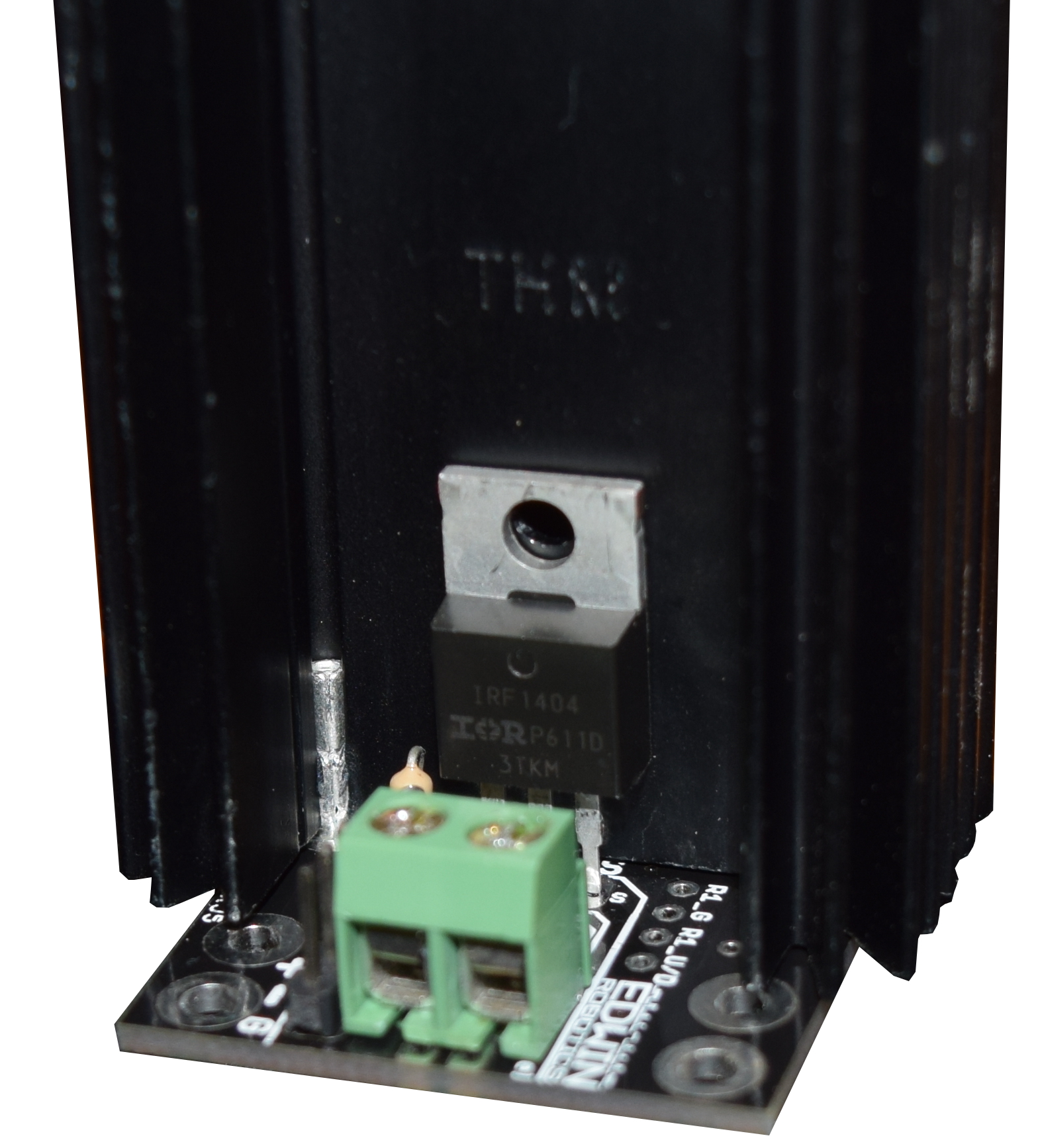
N Channel MOSFET with Heatsink
The P Channel also supports Heatsink. If you are using Heatsink with N Channel MOSFET then it is not possible to use P Channel MOSFET or vice versa. The Heatsink is not provided with the MOSFET Breakout PCB, you need to buy it separately if needed. If you are facing any issue or difficulty with the PCB, do let us know, our team will help you with all the issue, we are happy to hear from you, do let us know your feedback.
References:
- MOSFET types Image Source: Electronics Tutorials
- Heatsink Image Source: Sparkfun